


Exploring the Vital Role of PCBs in Modern Electronics
Print Circuit Boards(PCB) are the backbone of modern electronics, forming the basic element of any device. It provides a platform for connecting and arranging numerous electronic components into a compact and organised layout. The design flexibility of a PCB offers ease of scalability into electric circuits, making them suitable for a wide range of applications.
From smartphones to medical equipment, and from automotive systems to industrial machinery, PCBs play a pivotal role in shaping the modern technological landscape.
PCB Categories
Printed circuit boards are used for various purposes, and they fall into different categories: Class 1, Class 2, or Class 3. The classification of a PCB indicates its overall quality and reliability.
Class 1 boards are used in consumer electronics.
Class 2 boards are present in devices where reliability matters but isn’t critical. These devices aim to reduce failures.
Class 3 boards adhere to the strictest manufacturing standards. Failure of a Class 3 board can have serious consequences, such as on airplane boards where lives are at risk.
Key Stages in PCB Manufacturing
From Concept to Final Outlook
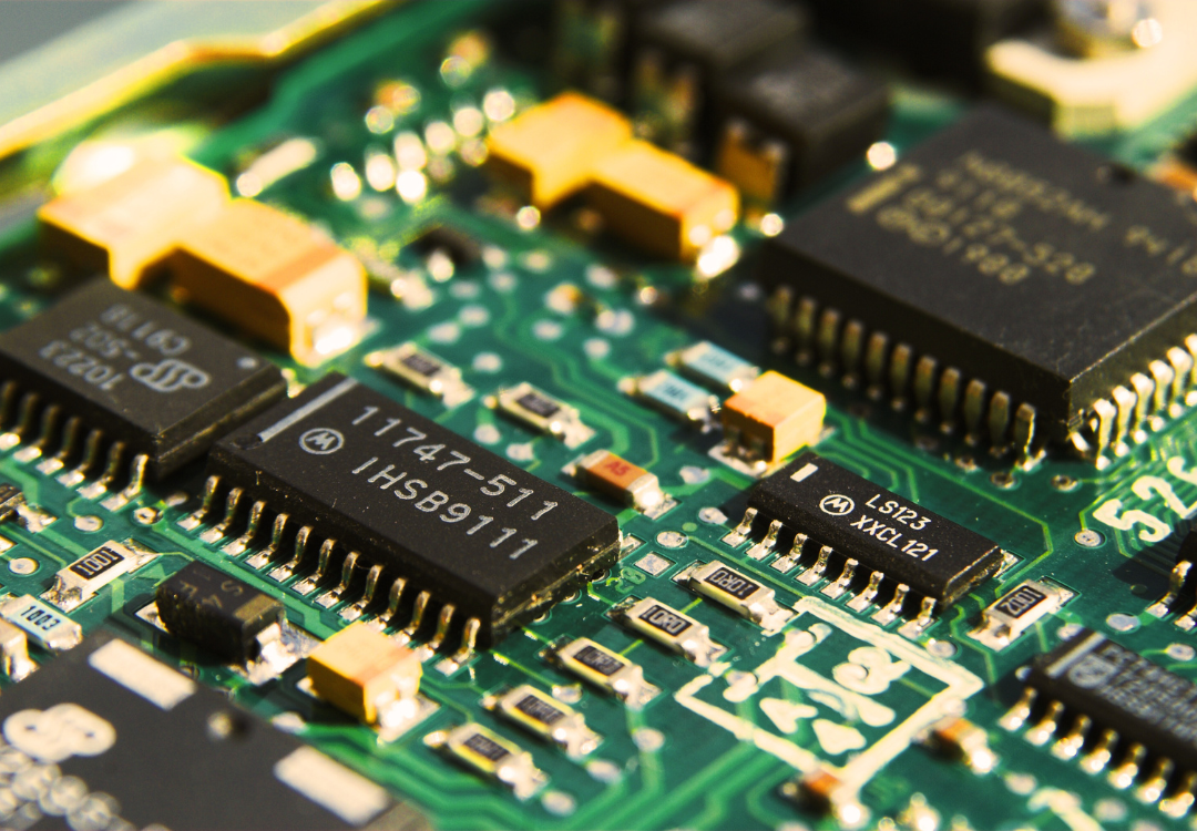
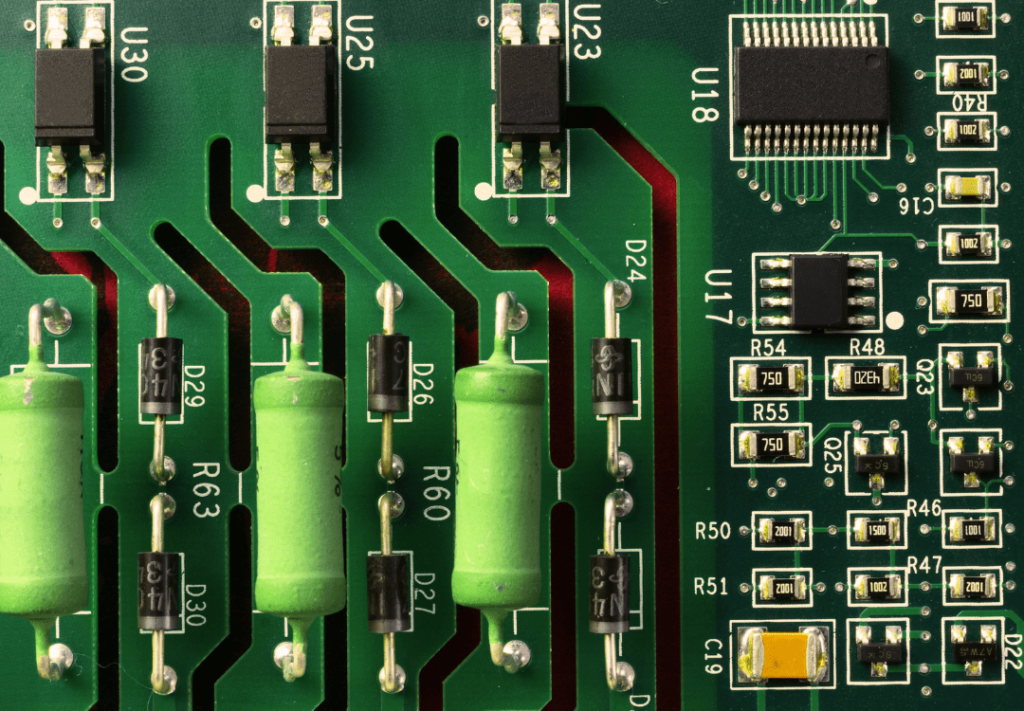
A printed circuit board (PCB) is a flat board made of non-conductive material like fibreglass that holds a solid structure with metal pathways called ‘traces’ and larger metal areas termed as ‘planes’.The pathways are conductive and are usually made of copper. Components are attached to the board using metal pads, which connect to the board’s circuitry. This lets components link together. PCBs can have one, two, or many layers of circuitry.
Creating CAD Library Components:
The initial phase involves crafting the CAD library components essential for the design. These include symbols, models for simulation, PCB footprints, and 3D models. After this, we build the circuit’s plan on a schematic. We use CAD tools to place symbols and connect them to form the circuit.
At the same time, we test the circuit using simulations to ensure it works as intended. Once done, the schematic details are sent to the layout tools.
PCB Fabrication: Unveiling the Manufacturing Process
Etching:
Most printed circuit boards are made by placing a layer of copper over the entire surface of the PCB substrate material, either on one side or both sides. This creates a copper-covered board. The next step involves removing the excess copper using subtractive methods.
Photoengraving Process:
Using a mask and chemical etching, the photoengraving process removes copper from the circuit board substrate.
The mask is made using a photoplotter, which takes the design from CAD PCB software. Sometimes, a lower-resolution mask is created with a transparency and laser printer.
Lamination:
PCBs consist of several thin etched boards which are bonded together through lamination. It involves aligning and bonding layers with heat and pressure, creating a strong structure. After cooling and inspection, the PCB is further processed. Lamination ensures reliable and high-performance multi-layer PCBs for electronics.
Drilling:
To connect different layers in a printed circuit board, small holes called “VIAS” are drilled. These holes are placed precisely drilled using automated drilling machines controlled by computer programs. These programs, called numerically controlled drill or excellon files, determine where and how big each hole should be in the design.
For specific needs, controlled depth drilling can be used to make holes in just one layer of the board, rather than going through all layers. This is done by drilling separate layers before putting them together.
Solder Plating:
The spots where electronic parts will be added, called pads and lands, get a special coating for easy soldering. Regular copper isn’t good for this, so a plating material is used to make soldering easier. In the past, they used tin with lead, but now they use newer materials like nickel and gold. These materials work well for soldering. Materials are applied to certain areas to prevent soldering from taking place there.
Silk Screen:
When the board needs logos, part numbers, or instructions, silk screening is used to put this on the outer surface. Where there’s enough space, the screened text can show component labels, switch settings, and extra details that aid in PCB assembly.
Testing:
Before putting components on, circuit boards are tested to ensure connections are right. In mass production, a bed of nails tester touches the copper areas to test. Computers control this test, sending a small current through each point on the tester to see if it’s correct.
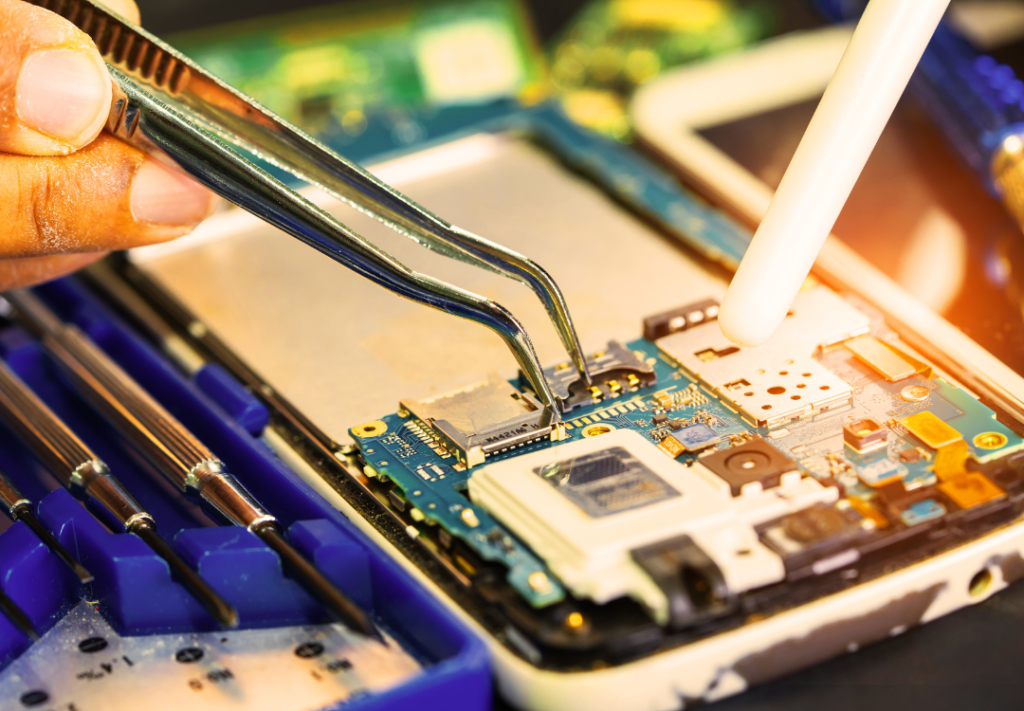
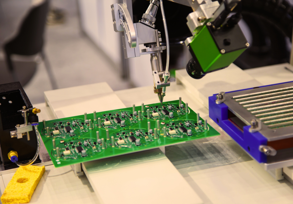
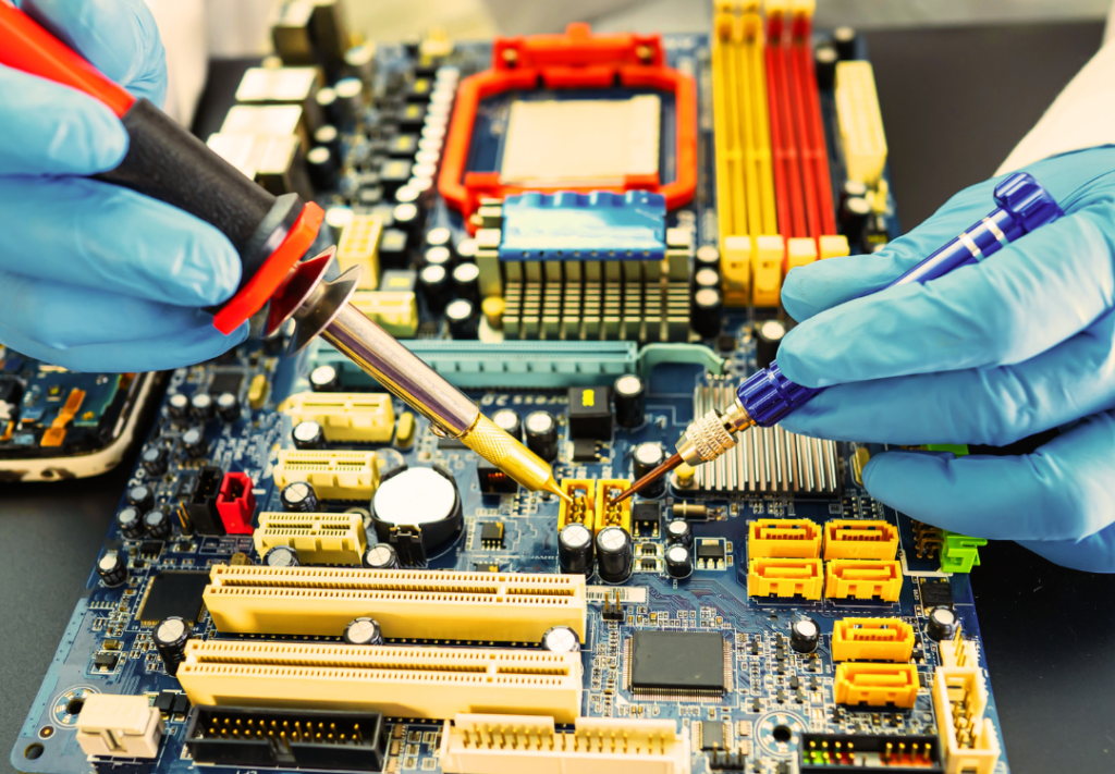
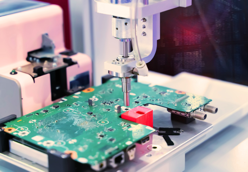
PCB Assembly Techniques
- Components Preparation
- Solder Paste Application
- Solder Paste Inspection
- Pick and Place
- Reflow Soldering
- Automated Optical Inspection
- Through Hole and Manual Assembly
- Wave Soldering of Through-hole
Component Sourcing: Finding the Right Parts for Your PCB
- Capacitors
- Resistors
- Inductors
- Diodes
- Microchips
- Transistors
- Potentiometers
- Transformers
- Integrated Circuits
- Sensors
Looking for a Reliable PCB Manufacturer?
We’re here to help with PCB Sourcing & Assembly of electronics interaction of your PCB design. Just share your PCB files or BOM, and our sales team will quickly provide you with a quote!
Karkhana.io is a flexible and scalable manufacturing solutions provider that can cater to all your manufacturing needs.
Our expertise in manufacturing can help you simplify and organise production processes according to your needs and industry. Whatever your requirements or goals maybe, we are dedicated to help you produce outstanding results with high quality whilst complying to the industry standards.
The flexible manufacturing services that fall under our spectrum enable us to fulfil client orders of all sorts, from small batches to large volumes. We also help our clients in solving complex product assembly and localisation setbacks.
If you’re looking for a PCB assembly and sourcing services that meet the technical capabilities whilst incorporating quality control systems, contact us today! Optimise your operations with Karkhana.io‘s expertise in manufacturing high performance components that meet industry standards.
Let us help you reach the optimal outcome for all your manufacturing requirements. To get started, simply email Alay Shah on alay@karkhana.io with your specifications or fill out the form below.
We cater to every manufacturing need across industries like Aerospace, Automation, Automobile, Defence, Drone, Energy, EVs, FMCG, General Engineering, Medical, Oil & Gas, Pharma, and Robotics.