


Ever wondered how a PCB is actually manufactured? A PCB is the backbone of any electronic component. The intricate technicalities involved to produce a PCB involves a number of critical steps. Each step requires precision, expertise, and attention to detail to ensure the final product meets performance, reliability, and safety standards.
Manufacturers strive to optimise their processes to meet the evolving needs of various industries. From consumer electronics to industrial machinery, PCBs are integral components in a wide range of products.
Step by step PCB Manufacturing
PCB Layout Design
Before manufacturing a PCB board, a design or layout is needed. This layout is like a circuit diagram, showing the path for each node. A specialized CAD (Computer-Aided Design) software is used to create these layouts. Software saves time and allows for easy last-minute changes. Once the design is final, it’s converted into the appropriate format for the manufacturer, usually Extended Gerber files. Gerber files represent schematic designs of the PCB design. Manufacturers then conduct a Design for Manufacturing (DFM) check to ensure it meets industry standards. During this phase, considerations such as component placement, routing, signal integrity, and manufacturability are addressed. After clearance, the layout is printed and ready for manufacturing.
Film Generation
The circuit diagram of each layer from the Gerber file is replicated onto a film. Inner layers use a negative film with black ink to depict the copper traces of the PCB, while outer layers use white ink for traces and black for etched areas. Additionally, the films are used to drill via holes.
Printing of Copper
The design from the film needs to be transferred onto the copper plates where the circuit will be printed. Each copper plate is combined with a core, cleaned, and treated with a special chemical called photoresist. The film with the circuit pattern is then placed over the copper plate and exposed to UV light. The light passes through the transparent parts of the film, hardening the photoresist chemical. Afterwards, any unhardened photoresist is removed using an alkaline solution. This process is how the circuit is printed onto the copper plate.
Layer Alignment along with Inspection
After individual cleaning, PCB layers undergo optical inspection and alignment using holes for alignment. A punch machine aligns layers, and optical inspection ensures fault-free assembly, crucial as corrections can’t be made later. AOI machines compare the PCB to the Gerber design for validation. Upon passing inspection, the PCB proceeds to the final manufacturing steps.
Etching
Etching involves removing excess copper from a copper plate, leaving behind only the desired copper traces. This excess copper is eliminated through chemical or mechanical means.
Lamination of the PCB Layers
In the PCB manufacturing process, defect-free layers are fused together through lamination. This occurs in two steps: lay-up and laminating. Fiberglass pieces coated with epoxy resin surround the PCB layers, containing copper traces. Layers are aligned and pressed using metal clamps and a special table. Pre-coated epoxy resin, substrate layers, copper foil, and more resin layers are stacked, followed by a copper press plate. The stack undergoes hard-pressing and laminating to fuse the layers with heat and pressure. After pressing, pins are removed, allowing the PCB to be extracted.
Drilling
Before drilling, an X-ray machine locates the drill spots, and guiding holes are drilled to protect the PCB stack. Computer-guided drills then make precise holes using the design file as a guide. After drilling, any excess copper at the edges is filed off.
PCB Plating
Once drilled, the panel undergoes plating, which chemically fuses all PCB layers. After thorough cleaning, the PCB is immersed in chemicals, coating it with a micron-thick layer of copper. This copper is deposited over the topmost layer and into the drilled holes, initially exposing the fiberglass substrate inside the panel. The copper bath covers the walls of the holes, gradually filling them.
Outer Layer Plating
Another layer of photoresist is applied, but only to the outer layer for imaging. Once coated, the outer layers undergo plating similar to the interior layers in the previous step. However, this time, the outer layers receive a tin plating to protect the copper on the outside layer.
Solder Masking
To prepare the panels for solder mask application, they undergo cleaning. After cleaning, ink epoxy and solder mask film are applied. The boards are then exposed to ultraviolet light to mark out areas for mask removal. Once unnecessary portions are removed, the PCB is cured in an oven to set the solder mask.
Silk Screening
During the finishing process, the PCB is plated with silver, gold, or HASL to facilitate soldering and protect the copper. Following plating, the PCB undergoes silk-screening to print essential information such as company ID numbers and warning labels. Once plated and silk-screened, the PCB proceeds to the final curing stage.
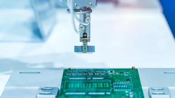
Testing
PCB undergoes functional testing to verify its performance and functionality. Various testing methods, including in-circuit testing (ICT), functional testing, and boundary scan testing, are employed to ensure that the PCB meets the specified electrical and operational requirements. Testing may involve applying electrical signals to the PCB and observing the responses to validate proper functionality.
Choose Karkhana.io for PCB Manufacturing Service
Each step involved in PCB manufacturing has to be conducted in a proper manner to avoid any defects and ensure high quality.
Karkhana.io is your one-stop solution to cater to all your electronic manufacturing requirements. With a network of 500 vetted and certified suppliers nationwide, well-versed in the intricacies of electronics integration and are trusted by top-tier companies, assuring you of optimal results!
Why do we stand out?
- Turnkey and contract manufacturing solutions
- Dedicated assembly lines for high-volume PCB assembly
- Global Sourcing of raw materials
- Integrated Quality Management System
Our flexible manufacturing services enable product efficiency and quality across orders of all sizes from small batches to large volumes, while offering box build solutions along with product localisation capabilities.
If you’re looking for an EMS provider that meets the technical capabilities, contact us today. Let us help you reach the optimal outcome for all your manufacturing requirements. To get started, simply email Pushpalaxmi Vanniyar at pushpalaxmi@karkhana.io with your specifications or fill out the form below.